Skip to content

[boards] Add Tuya WL2H-U (LN882H)#372

Open
Bl00d-B0b wants to merge 3 commits intolibretiny-eu:masterfrom
Bl00d-B0b:boards/add-wl2h-u
Open

[boards] Add Tuya WL2H-U (LN882H)#372
Bl00d-B0b wants to merge 3 commits intolibretiny-eu:masterfrom
Bl00d-B0b:boards/add-wl2h-u

Conversation

@Bl00d-B0b
Copy link
Copy Markdown

Summary

Add board definition for the Tuya WL2H-U Wi-Fi/BLE module based on the Lightning LN882HK chip.

Files added

  • boards/wl2h-u.json — board definition
  • boards/_base/pcb/wl2h-u.json — physical pinout (21 pads + test point TA9)
  • boards/variants/wl2h-u.c/.h — Arduino pin map

Hardware specs

  • CPU: ARM Cortex-M4F @ 160 MHz
  • RAM: 296 KB
  • Flash: 2 MB
  • Wi-Fi: 802.11b/g/n
  • BLE: 5.1
  • Module size: 15.8 × 20.3 mm
  • FCC ID: 2ANDL-WL2H-U
  • Vendor: Tuya

Pinout

Physical pinout verified against the official Tuya WL2H-U datasheet.

The module exposes 19 GPIOs (PA0–PA7, PA9–PA12, PB3–PB9). PA8 is not physically exposed.

Variant files were hand-generated from generic-ln882hki with PA8 removed — please regenerate with boardgen if needed.

Notes

  • Calibration of internal ADC temperature sensor: 25 + ((raw & 0xFFF) - 770) / 2.54 (empirically derived, community validation welcome)

Add board definition for the Tuya WL2H-U Wi-Fi/BLE module based on the
Lightning LN882HK chip.

- boards/wl2h-u.json: board definition (vendor: Tuya, FCC ID: 2ANDL-WL2H-U)
- boards/_base/pcb/wl2h-u.json: physical pinout based on official Tuya datasheet
- boards/variants/wl2h-u.c/.h: Arduino pin map (19 GPIOs; PA8 not exposed)

Pinout verified against the official Tuya WL2H-U Module Datasheet.
Module size: 15.8 x 20.3 mm, CPU: ARM Cortex-M4F @ 160 MHz, Flash: 2 MB.
@kuba2k2
Copy link
Copy Markdown
Member

kuba2k2 commented Apr 3, 2026

This doesn't look right.

obraz

Please verify your PRs before posting 🙂

@Bl00d-B0b
Copy link
Copy Markdown
Author

Bl00d-B0b commented Apr 5, 2026

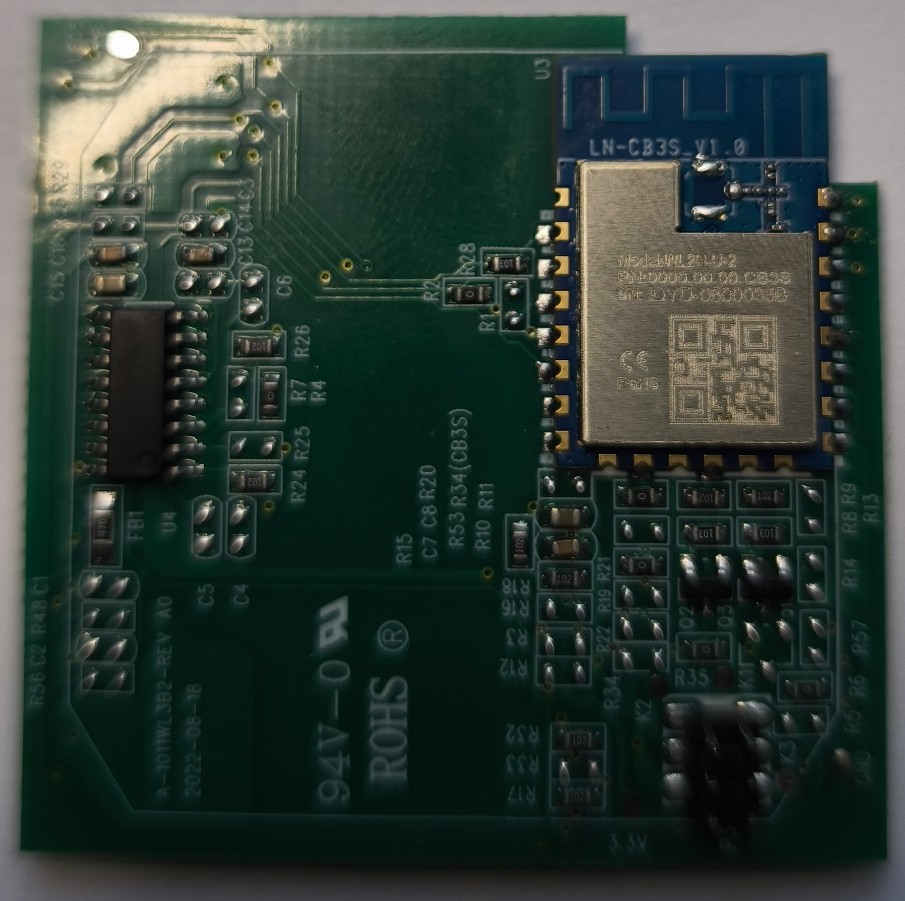
While testing this module, I found that the device actually uses an LN-CB3S V1.0 — a custom board in the same form factor as the Tuya CB3S (16×24mm, 22 pads), carrying a WL2H-U-2 chip (LN882H). It is not the standard Tuya WL2H-U module (15.8×20.3mm, 21 pads).

The LN-CB3S has a different pad assignment from WL2H-U — critically, VCC is at pad 8 and GND at pad 9, matching the CB3S layout exactly (unlike WL2H-U which has GND at pad 13 / VCC at pad 14). This was verified from a community schematic (elektroda.com topic4162022).

Hardware confirmed on the physical device (DS-101JL / BSEED WiFi Touch Light Switch 2 Gang):

  • Pad 1 / RST — not connected on this device
  • Pad 12 / A9 (GPIOA9) — pull to GND to enter flash/download mode ✓
  • Pad 15 / RXD1 (GPIOA3/U0RXD) and pad 16 / TXD1 (GPIOA2/U0TXD) — UART0 RX/TX ✓

Pin assignments in use:

Pin Function Direction Inverted
PA0 Backlight LED (red) Output yes
PA2 Indicator LED 2 (blue) Output yes
PA4 Indicator LED 1 (blue) Output yes
PA6 Relay 1 Output no
PA10 Status LED (blue) Output yes
PA11 Button 1 Input PULLUP yes
PB5 Relay 2 Output no
PB6 Button 2 Input PULLUP yes

I also have a DS-101JL 3-gang variant (BSEED WiFi Touch Light Switch 3 Gang) which uses the same LN-CB3S V1.0 module, but with a WL2H-U-3 chip. I will update this comment with the additional GPIO assignments once I finish reverse engineering it.

LN-CB3S V1.0 board with WL2H-U-2 module

This suggests it needs its own board definition with a CB3S-compatible PCB template. A few questions:

  1. Should this be a separate board entry (e.g. ln-cb3s) alongside wl2h-u in this PR, or a follow-up PR?
  2. What naming convention would you prefer — ln-cb3s, ln-cb3s-v1, or something else?
  3. Should the PCB template simply reuse pcb/cb3s.json with different IC pin mappings, or define a new pcb/ln-cb3s.json?

@kuba2k2
Copy link
Copy Markdown
Member

kuba2k2 commented Apr 5, 2026

  1. The wl2h-u board can stay in the same PR, but it must be fixed to reflect the correct form factor, as per the Tuya documentation.
  2. In this case the WL2H-U-2 marking doesn't really mean anything. It's probably either a misprint, or some other internal identification that clearly doesn't define the form factor of this board. The chip inside is LN882H, not "WL2H-U". Thus, the board should be named ln-cb3s-v1.0, which matches for example the already-existing t102-v1.1.
  3. Each board (boards/*.json) has its own "base" PCB definition (boards/_base/pcb/*.json), since each board has a different pinout. This alone pretty much requires a new pcb/ln-cb3s-v1.0.json file.

Sign up for free to join this conversation on GitHub. Already have an account? Sign in to comment

Labels

None yet

Projects

None yet

Development

Successfully merging this pull request may close these issues.

2 participants